Difference between revisions of "PENELOPE"
m |
(→PENELOPE - Companion Exciter to Mercury) |
||
| Line 1: | Line 1: | ||
==PENELOPE - Companion Exciter to Mercury== | ==PENELOPE - Companion Exciter to Mercury== | ||
| + | 3rd May 2007 - Alpha PCB working, V2 PCB presently being layed out, block diagram updated to reflect latest changes. | ||
| + | |||
19th April 2007 - Alpha 1 kits sent to Penelope testers! | 19th April 2007 - Alpha 1 kits sent to Penelope testers! | ||
| Line 63: | Line 65: | ||
A block diagram is shown below. | A block diagram is shown below. | ||
| − | [[Image:DUC- | + | [[Image:DUC-v10.jpg]] |
Revision as of 04:29, 3 May 2007
PENELOPE - Companion Exciter to Mercury
3rd May 2007 - Alpha PCB working, V2 PCB presently being layed out, block diagram updated to reflect latest changes.
19th April 2007 - Alpha 1 kits sent to Penelope testers!
14th April 2007 - Added Alpha 1 Notes at bottom of this page to track errors and lessons learned.
13th April 2007 - Bare PCBs received! Photo below.
5th April 2007 - Update.
- PCB files : http://www.hamsdr.com/personaldirectory.aspx?id=549
- TAPR Board Approved Penelope Alpha 1 funding! Five (5) sets of parts and PCBs ordered today.
1st April 2007 - Added Verilog block diagram.
30th March 2007 - Update. PCB Layout edits and corrections : (replaced 05 Apr 2007)
29th March 2007 - Update. PCB Layout has many minor edits and corrections : (replaced 30 Mar 2007)
28th March 2007 - Update.
- Block diagram updated to reflect prototype PCB layout.
- Updated Alpha schematic (XA13) for Penelope is here : http://www.hamsdr.com/personaldirectory.aspx?id=534
- Initial PCB Layout posted here: (replaced 29 Mar 2007)
- Initial BOM posted here: http://www.hamsdr.com/personaldirectory.aspx?id=536
17th February 2007 - Update. Block diagram updated to reflect latest schematic.
14th February 2007: Preliminary Alpha schematic (XA8) for Penelope is here : (replaced 28 Mar 2007)
8th February 2007 - Update. Block diagram updated to reflect current Breadboard design.
7th February 2007 - Update. Block diagram updated to reflect design feedback. Breadboard built, tested and working. Prototype PCB layout started.
3rd February 2007 - Initial Specification
The Atlas compatible transmitter will use Digital Up Conversion (DUC) techniques and process the I and Q signal from the PC (or Sasquatch DSP board) directly without the need for a sound card.
Some of the planned features include:
 1.8 - 55MHz frequency coverage
 0.5W pep output
 Low level transverter output
 AM, C-AM, FM, CW, PSK etc
 RF phase and magnitude outputs for future Envelope Elimination and Restoration (EER) power amplifier
 Open drain FET for PTT control of external amplifiers
 Seven open collector outputs for Linear, relay etc control,
 Solid state antenna changeover relay for fast QSK.
 Optional on board microphone ADC or use with a Janus card
 Frequency options:
  o On board high performance 125MHz crystal oscillator
  o External 125MHz source
  o On board oscillator can be phase locked to 10MHz reference e.g. Gibraltar
  o On board 10MHz OCXO/TCXO  option
 FPGA based DUC enabling future code upgrades
 USB interface to PC via Ozy board
 I and Q balanced adjustment not required due to digital generation of RF waveform
 ADC for ALC or PA linearization etc.
 ALC processed in the FPGA to avoid  delays associated with PC processing
Lyle, KK7P, has kindly agreed to lay out the PCB. Please provide feedback, comments and feature requests via the hpsdr reflector.
Phil... VK6APH
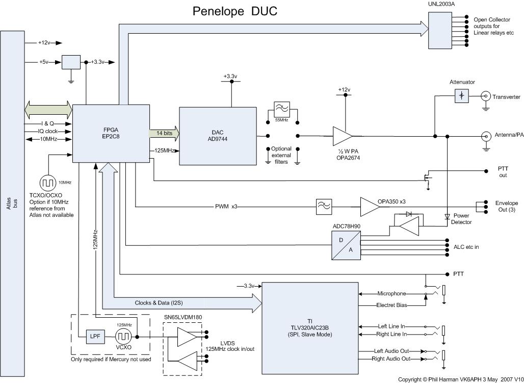
A block diagram is shown below.
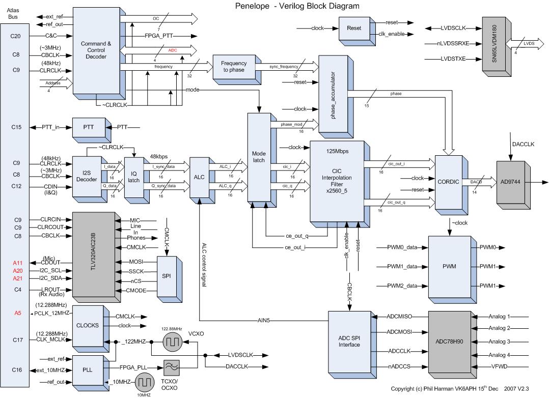
Verilog block diagram
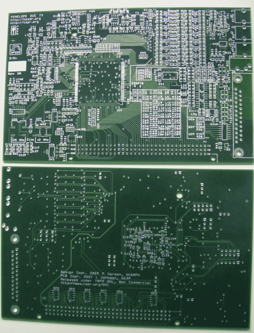
Photo of Unpopulated Alpha 1 Boards
Alpha 1 Notes:
This section will contain notes as we build and learn the mistakes made on Alpha 1.
14th April 2007: EP2C8 pinout error. Pin 36 mistakenly made an IO, it is GND. Cut trace near pin 36. Add short jumper pin 36 to pin 38 (GND). Add short jumper trace side of cut to pin 41. Use pin 41 as DACCLK.
23rd April 2007:
- U31 pin 3 not connected to 3V3. Jumper to U36.
- L27 doesn't pick up 3V3. Jumper to U36.
- U11 pin 2 not grounded. Jumper to C41 or C50.
- PCB silkscreen doesn't show pin 1 on Hittite switches. U9 - lower left. U12 - upper right. Right hand bank of filter switches: lower right. Left hand bank of filter switches: upper left.


