Difference between revisions of "HERCULES"
(Added Hercules Component Layout) |
(Added instructions for building interconnect cable - Penny/Ant. switch/Hercules) |
||
| Line 110: | Line 110: | ||
19. Mate the circuit board to the heatsink and tighten all screws including the hardware from plastic bag in the parts kit. | 19. Mate the circuit board to the heatsink and tighten all screws including the hardware from plastic bag in the parts kit. | ||
| − | 20. Assembly Instructions for the Hercules 100W_PA Display module: | + | 20. Assembly of the Cable from Penelope to the Antenna Switch and to the 100W_PA: |
| + | |||
| + | |||
| + | A flat ribbon cable is used for the connection from Penelope to the antenna switch and to the PA. | ||
| + | |||
| + | There is a separate document which contains the netlist for the cable from Penelope to the antenna switch and further to the PA. | ||
| + | Please note that pin 13 (on the other end as pin 1) on the DSUB25 connectors goes to pin 1 of J10 on the PA. | ||
| + | |||
| + | I suggest that you mount the DSUB25 connectors on the cable with the color marked lead going to pin 13 and not to pin 1 as you would normally do it. Thus the marked lead ends on Pin 1 of the 16 pole connector to the PA. | ||
| + | |||
| + | You should start to connect one DSUB25 connector on one end of the cable. The colored lead of the cable shall be connected to pin 13 of the DSUB25. This end is to be connected to Penelope. Please check that your cable leaves the connector in the counter direction to the antenna switch. After a 180° turn you clip the plastic cable retainer on this connector. The cable now goes in direction to the antenna switch. In the correct distance you press the second DB25 connector on the cable. The cable goes through this connector. The orientation of this second connector has to be the same as for the first: colored lead to pin 13. The last connector is a 16 pole female header that is pressed on the cable with the colored lead connecting to pin1. Pin 1 is marked on the housing with an arrow. The last 9 wires of the cable are strapped off from the cable for a length of about 2-3cm. (1 inch). Either you cut the not used wires or you bend it backwards and isolate it. Again you must take into account that the connector to the PA has a cable retainer which needs a 180° turn of the cable direction. | ||
| + | |||
| + | |||
| + | |||
| + | 21. Assembly Instructions for the Hercules 100W_PA Display module: | ||
Note #5:The topside of the pcb is marked “BS” | Note #5:The topside of the pcb is marked “BS” | ||
Revision as of 06:40, 27 February 2010
HERCULES
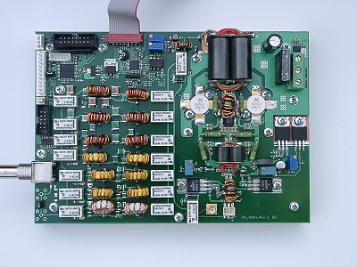
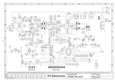
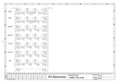
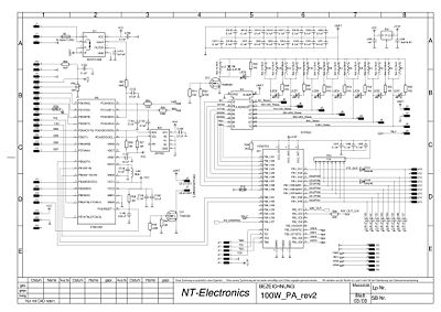
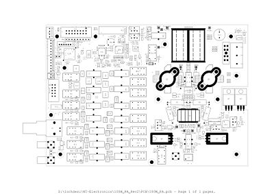
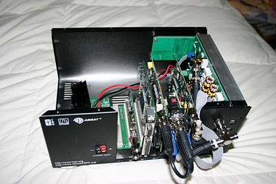
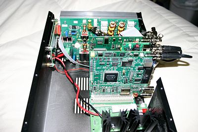
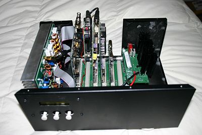
This amplifier is designed to work with the current HPSDR Penelope transmitter assembly to amplify the signal of max. 500 mW to 100 Watts RF output. It was designed to operate from 160m up to and including 6m in all HF Amateur bands in all modes. See Photos 2, 3, & 4 for as built schematic drawings.
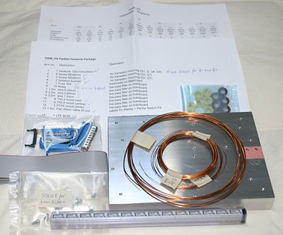
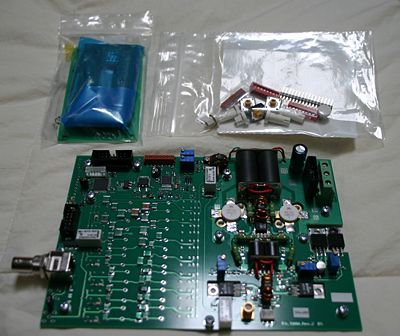
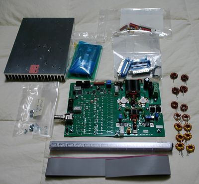
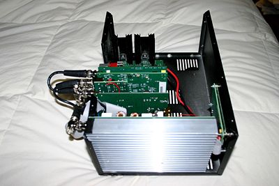
All parts are included including a drilled and tapped 185 X130 X 25 mm heatsink (see photo above). The parts are mailed in two packages. The first package has the heatsink, hardware, toroids, wire, fuse, flat ribbon cable, ribbon connectors, and relays. An overall enclosure is not included.
Functions and Features:
The amplifier uses a four layer circuit board, which makes possible optimum impedance match of all the HF circuit board lines. The Amplifier is installed onto an Aluminum heat sink by the user. Dimensions LxWxH are185 x 130 x 50mm. Cooling fans may be required by the user depending upon type of mounting and the planned duty cycle of usage. Connections to the optional PWR/SWR meter and the HPSDR Pentelope transmit exciter board starts on the Amplifier's printed circuit board via a single flat strip cable. By programming the on board CPLD, additional interfaces can be implemented.
Operating voltages are 12-14 Volts with current input to a maximum of 25 Amperes, HF-power output is 100W PEP on 160-10m, and 50W on 6m.
Frequency range: 1.8MHz to 52MHz with 7 bandpass filters for 160m, 80m, 60/40m, 30/20m, 17/15m, 12/10m and 6m. Designed for max. transmission and min. return, the band pass filters use single-aperture cores and SMD mica capacitors with high Q and min. losses. The bandpass filters can alternatively be used only in the transmit mode or in the transmission and receive mode. The selection takes place via selection of a CPLD program by means of a circuit board jumper.
Monitoring of the operational data is accomplished by using an Atmega CONTROLLER and the data is indicated on an optional 4 parameter LCD. The selection of limit values and selection of the display mode take place via 3 keys under the display as follows:
• Temperature measurement at the heat sink to the nearest degree C
• Set point for the start-up of cooling fans is adjustable from 50 to 80°C
• Set points for the limits for switch off the amplifier is adjustable from 60 to 90°C
• Fan Hysteresis is 10°C (in firmware).
• Indicator for power input 0-25A.
• Current limit for switching off Amplifier adjustable from 7 to 25A
• FWD_PWR measurement in Watts
• REV_PWR measurement in Watts
• SWR measurement to one right-of-comma position.
• Limit for switching the final stage off adjustable with SWR greater than 1,5 to 3
Hercules Build Instructions:
Note #1 Leave all screws and nuts installed loosely on the main circuit board as they are. The nuts will be used as circuit board spacers when assembled to the heatsink.
Note #2 After the winding the filter single-aperture cores, they should be checked against the specified inductances, if a L-measuring instrument is present. Inductance can be changed by pushing together or even distributing on the single-aperture cores around approx. 10%. In the case of doubt indicated inductances are valid before the numbers of turns. The wire provided is not solderable, i.e. it must be stripped. It should be stripped up to the single-aperture core, so that the wires can be soldered briefly.
1. Wind 28 turns of .35 mm dia. enameled wire on to a (red) T50-2 toroid. Cut and tin the leads at about 1/2" below the toroid. This coil will be designated L1 at 4 UH.
2. Wind 28 turns of .35 mm dia. enameled wire on to a (red) T50-2 toroid. Cut and tin the leads at about 1/2" below the toroid. This coil will be designated L2 at 4 UH.
3. Wind 17 turns of .8 mm dia. enameled wire on to a (red) T50-2 toroid. Cut and tin the leads at about 1/2" below the toroid. This coil will be designated L3 at 1.5 UH.
4. Wind 19 turns of .8 mm dia. enameled wire on to a (red) T50-2 toroid. Cut and tin the leads at about 1/2" below the toroid. This coil will be designated L4 at 1.8 UH.
5. Wind 15 turns of .8 mm dia. enameled wire on to a (red) T50-2 toroid. Cut and tin the leads at about 1/2" below the toroid. This coil will be designated L5 at 1.2 UH.
6. Wind 15 turns of .8 mm dia. enameled wire on to a (red) T50-2 toroid. Cut and tin the leads at about 1/2" below the toroid. This coil will be designated L6 at 1.3 UH.
7. Wind 10 turns of 1.0 mm dia. enameled wire on to a (yellow) T50-6 toroid. Cut and tin the leads at about 1/2" below the toroid. This coil will be designated L7 at 620 nH.
8. Wind 10 turns of 1.0 mm dia. enameled wire on to a (yellow) T50-6 toroid. Cut and tin the leads at about 1/2" below the toroid. This coil will be designated L8 at 620 nH.
9. Wind 9 turns of 1.0 mm dia. enameled wire on to a (yellow) T50-6 toroid. Cut and tin the leads at about 1/2" below the toroid. This coil will be designated L9 at 430 nH.
10. Wind 9 turns of 1.0 mm dia. enameled wire on to a (yellow) T50-6 toroid. Cut and tin the leads at about 1/2" below the toroid. This coil will be designated L10 at 430 nH.
11. Wind 7 turns of 1.0 mm dia. enameled wire on to a (yellow) T50-6 toroid. Cut and tin the leads at about 1/2" below the toroid. This coil will be designated L11 at 300 nH.
12. Wind 7 turns of 1.0 mm dia. enameled wire on to a (yellow) T50-6 toroid. Cut and tin the leads at about 1/2" below the toroid. This coil will be designated L12 at 300 nH.
13. Wind 10 turns of 1.0 mm dia. enameled wire on to a (white) PTFE toroid. Cut and tin the leads at about 1/2" below the toroid. This coil will be designated L17 at 137 nH.
14. Wind 10 turns of 1.0 mm dia. enameled wire on to a (white) PTFE toroid. Cut and tin the leads at about 1/2" below the toroid. This coil will be designated L18 at 143 nH.
15. Solder the 14 remaining relays to the main circuit board.
16. Solder and close trim L-1 to L12, L-17 and L-18.
Note #3 When the assembling of the printed circuit board on the radiator box the same is to be considered as with the disassembly only in reverse order. The radiator box surface must be freely of foreign parts, in particular under the power transistors. Otherwise the heat dissipation is handicapped. A view laterally by the gap between printed circuit board and radiator box is helpful to determine over whether the power transistors flat mounts. It may not be visible a light gap. When finally last screwing on thermal compound can (in thin layer!!) the heat coupling of the power transistors improve. This is meaningful however only for the final stage transistors.
17. Clean off any solder flux left on the circuit board from steps 15 and 16 above and inspect work so far.
18. Apply thermal compound (example: Antec Formula 5... Silver Bullet) to the heat sink surfaces of the transistors (4). Do not apply the compound to the two transistors that mount to the insulating pads.
Note #4 When screwing the fixing bolts in an alternating can solve short release around a half revolution the blocking of the mother on the radiator box and make then further screwing in possible. Also holding of the printed circuit board down against the mother can be helpful. The 8 transistor fixing bolts are screwed in only last and tightened firmly however moderately and evenly.
19. Mate the circuit board to the heatsink and tighten all screws including the hardware from plastic bag in the parts kit.
20. Assembly of the Cable from Penelope to the Antenna Switch and to the 100W_PA:
A flat ribbon cable is used for the connection from Penelope to the antenna switch and to the PA.
There is a separate document which contains the netlist for the cable from Penelope to the antenna switch and further to the PA. Please note that pin 13 (on the other end as pin 1) on the DSUB25 connectors goes to pin 1 of J10 on the PA.
I suggest that you mount the DSUB25 connectors on the cable with the color marked lead going to pin 13 and not to pin 1 as you would normally do it. Thus the marked lead ends on Pin 1 of the 16 pole connector to the PA.
You should start to connect one DSUB25 connector on one end of the cable. The colored lead of the cable shall be connected to pin 13 of the DSUB25. This end is to be connected to Penelope. Please check that your cable leaves the connector in the counter direction to the antenna switch. After a 180° turn you clip the plastic cable retainer on this connector. The cable now goes in direction to the antenna switch. In the correct distance you press the second DB25 connector on the cable. The cable goes through this connector. The orientation of this second connector has to be the same as for the first: colored lead to pin 13. The last connector is a 16 pole female header that is pressed on the cable with the colored lead connecting to pin1. Pin 1 is marked on the housing with an arrow. The last 9 wires of the cable are strapped off from the cable for a length of about 2-3cm. (1 inch). Either you cut the not used wires or you bend it backwards and isolate it. Again you must take into account that the connector to the PA has a cable retainer which needs a 180° turn of the cable direction.
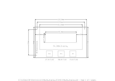
21. Assembly Instructions for the Hercules 100W_PA Display module:
Note #5:The topside of the pcb is marked “BS” The bottom side is marked with “LS”
On the topside the following are assembled: 3 push buttons, 1 header-16pole, for the display (near the push buttons). The connector at the top boarder of the monitor circuit board is provided for different displays which have the connector on the upper side and is not used for this display. The shorter pin side of the header is soldered to the pcb and the display module is plugged on the longer pins and soldered. This gives enough stability for the display module. However you can fix the upper side of the display module with one or two dots of silicon glue.
On the bottom side of the pcb is assembled a Tantalum capacitor C1. The marked side of C1 is the +pole that is connected to VCC on the board (+5 volts). Also install the very small 100nf 0805 SMD capacitor C2 that is in the component package for this board (not packaged or on tape in my kit - it is so small it could get misplaced easily if not placed on a length of of masking tape to secure it). The red 16-pole MicroMatch connector is keyed on one end. You must mount this connector with the keyed end (pin 1) pointing toward the top of the monitor circuit board. If for some reason you mount this connector upside down (I did)it will be very difficult to repair successfully. Use a Chip Quik SMD Solder/Desolder kit and follow the directions in the package.
22. Assembly of the display cable.
First you should verify how long your cable from the display to connector J12 on the main board has to be. It depends on your specific mounting in a housing. Cut the desired length from the supplied cable. Take care that you cut it with a sharp scissors or knife. Use 16 leads of this piece of cable beginning from the color marked lead. The resting 9 leads are pulled off from the cable and are no longer used. The male connectors are pressed onto the cable that the marked lead of the cable shows to pin1 of the connectors i.e. by means of a bench vise. Take care not to damage the coding nose while using the vise. The nose must stay outside the vise jaws. Also take care that the cable exits the connector in the correct direction fitting your mounting. I must admit here that I tried to use a pair of pliers to do the insulation displacement closing of the connector on the ribbon cable and destroyed 4 connectors before I used a bench vise with success, Digi-Key has the connector in stock as part number A99458CT-ND "CONN MALE-ON-WIRE 16 POS 28 AWG. I ordered 10 and have 6 of the parts left over if someone needs one or two.
23. Display tests
Connect the display to the mainboard and connect 12V to the green connector J1 on the mainboard which needs not be mounted onto the heatsink for this test. The Pins are marked with +12V and GND on the pcb. Insert the fuse into the holder next to J1 and the display should then show 2 lines with FWD and REV Power and current 0A. You can adjust the display contrast with pot VR4 which is next to the display connector J12.
The push buttons are called: left : - (minus) middle: + (plus) right: OK or ENTER
With + and – you can change the displayed pages between power/current and temperature.
24. Testing the power amplifier circuits: Before attempting to activate the transmitter via the MOX command on Power SDR, Potentiometer VR1, VR6, VR2 (quiescent current indication) as well as VR3, VR5 (power indication) must be set to the complete anti-clockwise direction (to a complete stop turn). The rotation stop of the Potentiometers can be determined only by increased resistance to rotation. If the spindle is kept turning, the Potentiometer can be damaged. If after first application of power no announcement on the display appears, the contrast must be adjusted with Potentiometer VR4. Must be adjusted to a high-contrast announcement without background density effected.
25. Amplifier Bias ajustments:
Ajusting the quiescent currents of driver and final stage transistors: Place an Ammeter capable of reading current to the nearest 10 ma into the 12V supply line and activate the transmit mode with no RF on the input SMA connector (disconnect RF from Penelope), the following current should be observed (if you get substantially higher currents, recheck to see that all Potentiometers are set to the complete ant-clockwise positions):
Without display, (invalid EEPROM data) 50 mA
With display 0.23 A
Adjust the quiescent (bias) current for each both drivers to 50 mA: VR1 regulates the quiescent current for Q4 (adjust total current to 0.28A), VR6 regulates the quiescent current for Q5 (adjust total current to 0.33A).
Final stage bias is to be set at 500 mA: VR2 regulates the quiescent current for both final stage transistors Q1, Q2. Adjust VR2 to the total value of current of 0.83 A (only if the driver bias has been set as specified prior to this adjustment).
26. At this point you have two choices on how to connect Hercules into your system:
A. Place Hercules between Pentelope and the antenna switch.
or
B. Place Hercules between the antenna switch and the Antenna tuner.
I have tried both placements and have chosen "B" option to better filter the Mercury RF input, and to keep the power level lower in the antenna switch. I think jumper 10 on the Amplifier should be changed to effect the control system for the "A" or "B" mode change, but in documentation seen to-date, this is not defined as to function and setting.
