MERCURY
MERCURY - 0-30MHz Direct Sampling Receiver
The project leaders for the Mercury board are Phil Harman, VK6APH and Philip Covington [1], N8VB. The Mercury design will incorporate many design features of the QuickSilver QS1R [2] prototype also designed by Philip Covington, N8VB.
Perhaps the most exciting of all the modules, the Mercury board will enable direct sampling of the 0-65MHz spectrum. Based on a Linear Technology LTC2208 130MSPS 16-bit A/D converter [3] the board will contain it's own FPGA to undertake Digital Down Conversion (DDC) to 250 kSPS or less for transfer over the Atlas bus to the USB interface on the OZY board.
MERCURY will downsample in its own Altera Cyclone III FPGA, not unlike the USRP [4].
There will be an option to upgrade to the LTC2209 170 MSPS 16 bit converter from Linear Technology.
Update 24th August: Alpha XA12 Schematic posted: http://www.hamsdr.com/dnld.aspx?id=875
Update 23rd August 2008: Mercury Alpha 2 prototypes have been tested. A minor issue arose which required a modification to the PCB layout. Alpha 3 PCBs are due Friday August 29th for commercial attachment of the ADC, preamp and FPGA chips. Final assembly of two Alpha 3 prototypes will then be done by the testers and measurmeents taken. We really hope this is the last PCB turn!
Update 10th July 2008: Mercury Alpha 2 prototypes were commercially assembled as a test run for release. One minor problem was found on a PCB footprint and has been fixed in the layout. The boards have passed functional testing (thank you, Scotty!) and are enroute to the Alpha test team!
Update 19th June 2008: Rev B PCB Files (corresponds to Alpha XA9 Schematic) posted: (contains design review details, but not complete manufacturing data pending board testing pending changes) http://www.hamsdr.com/personaldirectory.aspx?id=831
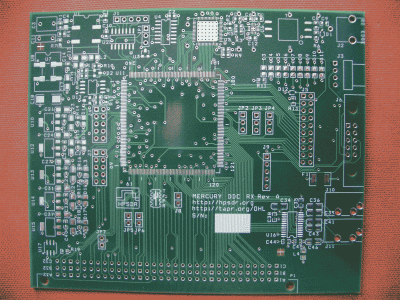
Update 16th April 2008: Alpha PCBs and parts kits arrived. Here is a photo of the bare PCB:
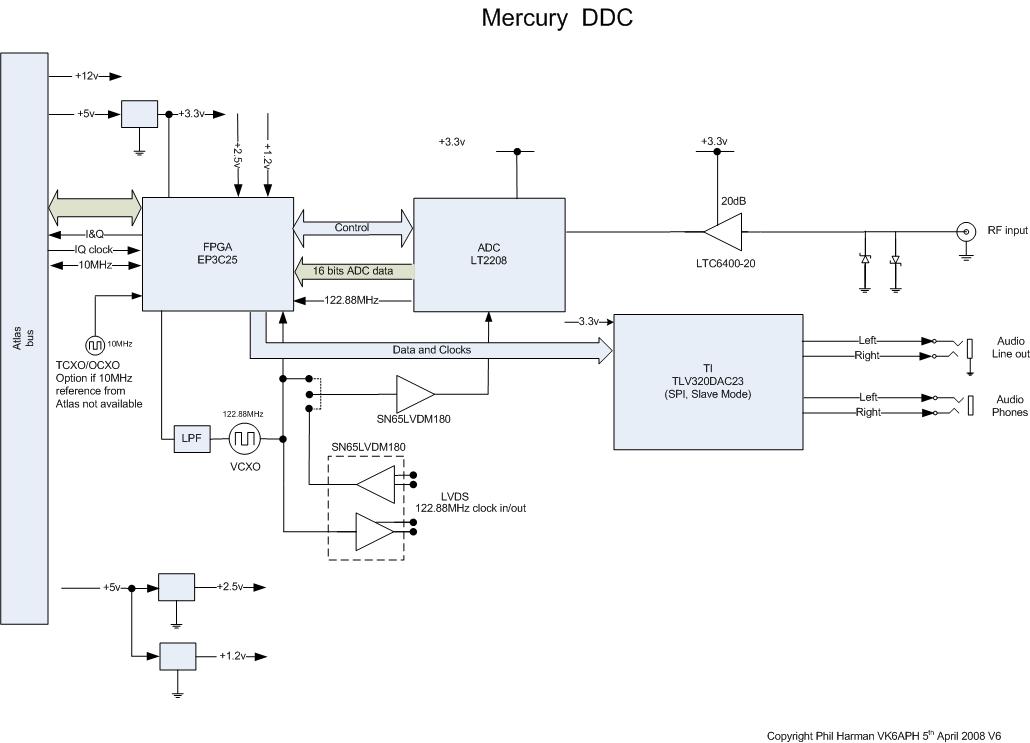
Update 5th April 2008: Updated block diagram to represent current schematic.
Update 18th March 2008: TAPR has agreed to fund the Mercury development proposal.
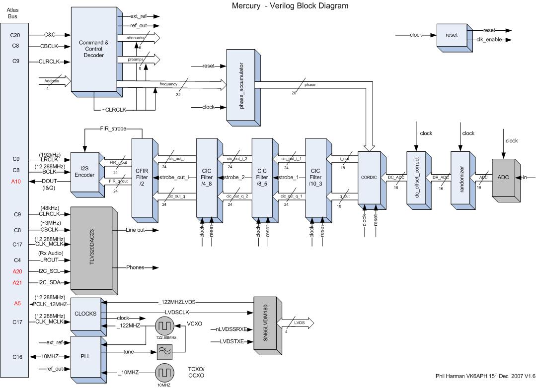
Update 24th May 2007: Block diagram of Verilog code added.
Update 3 May 2007: Block diagram updated. Lyle KK7P has offered to lay out the PCB.
Update 1 April 2007: Block diagram added to Wiki.
Block diagram of Alpha design
Block diagram of Prototype Verilog code
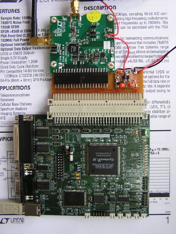
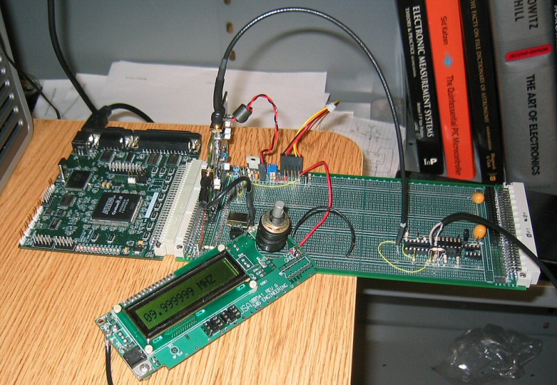
This is a photo of an LT2208 evaluation board connected to an Ozy board. (The little board to the right is a 3.3v regulator)
(Above) Initial Mercury prototype by Phil Covington, N8VB
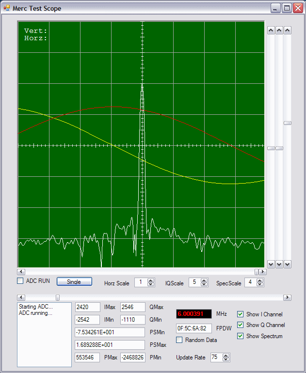
(Above) Mercury spectrum analyzer software written by Phil Covington, N8VB
Update 28th December 2006.
The V2 Ozy board has double the number of LEs of the previous board so provides a little more room to experiment with the CIC filters. I've managed to fit a 4 section decimate by 512 CIC filter in the FPGA that provides an approximately 195kHz 24bit data stream to PowerSDR. By making the data stream compatible with PowerSDR we can use all the features of that code to evaluate the LT2208. Bill, KD5TFD, added code to PowerSDR to send the current frequency over the USB link to Ozy and that is decoded and applied to the CORDIC NCO in Mercury. That way when PowerSDR is tuned Mercury follows.
As per the calculations below the LT2208 does not require a preamp below 20m. I added a 20dB preamp for the higher bands. At the moment I'm using my ATU as the only form of input filtering and so far there appears to be no strong signal problems.
Today I added a PWM DAC to the FPGA that operates at approximately 48kHz. This allows me to listen to the output of the receiver. My initial reactions are that this is going to be a very good receiver! Whilst the CORDIC NCO spurs are a little higher than I would like there are very large sections of all bands where there a no spurs at all. We have a volunteer working on improving the spur performance. Due to the large number of LEs needed in the FPGA to get acceptable filtering performance we are evaluating alternative technologies to implement the DDC.
Phil...VK6APH
Merc Spec/Scope added Sept 7, 2006
1th August 2006. Preliminary measurements are as follows:
        Maximum input level =   +9dBm
              MDS(500Hz BW) = -120dBm
Since the input transformer on the evaluation board is 1:1 then these results agree with Nyall's calculations below.
15th August 2006. Many thanks to Nyall Davies, G8IBR for providing these calculations. Nyall has many years experience in developing DSP based radar systems and his input and expertise is greatly appreciated.
Mercury - Theoretical Performance
 LT2208 clocking at 100 MHz
 Input level 1.5 Volts peak to peak mode.
 SFDR is quoted as 100 dB typical from 5 to 30 MHz. This figure will be used for IP3 calculations.
 Input impedance - balanced 200 Ohm.
IP3 of A/D converter
Thus input power 1.5 dBm for full scale. The A/D is specified at -1 dB full scale, i.e. 0.5 dBm. At this power the maximum third order spurious is 0.5 - 100 = 99.5 dBm From the IP3 diagram the IP3 is 50.5 dBm (54 with 2.25 Vpp input)
Noise figure of A/D converter
The signal to noise ratio of the A/D converter is typically 75.2 dB at 30 MHz and 75.3 at 5 MHz suggesting that we can take it as being evenly spread across the sampling bandwidth. Normally with a single A/D the Nyquist bandwidth is half the sampling frequency but we will be generating phase and quadrature signals so the noise is spread across the full sampling bandwidth. (It can be thought of as 2 samples.) the noise then will be bandwidth limited in the signal processing thus reducing the noise referred back to the input of the A/D by the ratio of the sampling bandwidth to the final bandwidth.
For an SSB bandwidth the noise referred A/D input
       = -75.2 dB below -1 dB FS - 10 Log(100 MHz/2.4 kHz)
       = -122.4 dBm
Now KTB is -140 dBm thus the noise figure at the A/D input
= 17.6 dB
For 500 Hz bandwidth the noise referred to A/D input
      = -75.2 -1 - 10 Log(100MHz/500 Hz)
      = -129.2 dB
Thus the noise figure is the same as noise figure is not a function of bandwidth.
LOSSES - NOTE this has assumed no signal processing losses. Signal processing losses will add directly to the noise figure. These could consist of filter weighting loss, truncation losses and clock and A/D jitter.
LOSSES
Mixer. The digital mixer will have an insertion loss of 3.9 dB so the numbers in the processing will be that amount lower than those coming out of the A/D. Normally there is a 3 dB signal to noise loss due to the image noise from the front end amplifier. As we will be sampling I & Q we will effectively have an image rejection mixer thus no S/N loss is put in for the mixer.
Clock and A/D jitter
The aperture jitter of the LT2208 is 70 fs or 0.07 picoseconds For the sake of fairness we will allow the clock jitter to match the A/D aperture jitter. This can be translated into SSB phase noise and requires an oscillator as follows
      300 Hz off carrier              -110 dBc/Hz
      2000 Hz off                     -139 dBc/Hz
      5000 Hz off                     -142 dBc/Hz
This is not unreasonable for a good crystal oscillator. The effect is worse at higher frequencies according to the formula
SNR=20 Log(2 pi fin trms)
Where fin is the input frequency and trms is the rms aperture jitter.
This works out at 95 dB at 30 MHz. This appears somewhat meaningless, as the noise distribution will follow the spectrum of the clock. It does mean that we will have an effect similar to reciprocal mixing that will be worst at 10 m.
Truncation losses should not be a problem with a 32 bit system but the word growth in the CIC filters is large. (Number of stages raised to the power of the decimation. As these are usually equal it is NN.) This means that several filters with lower numbers of stages and decimation ratio are usually cascaded and lower bits dropped off.
Weighting loss would appear to be negligible with FIR filters giving one output sample for each input sample but if used for decimation with one output for every input there may be a weighting loss. I will presume that there are no S/N losses associated with the CIC filters, as I can find no reference to them but I have some reservations.
If FFT processing is used, a weighting loss can be calculated.
Without knowing the algorithms I would suggest from experience and gut feeling that we should think in terms of adding 3 dB to the previously calculated noise figure and call it 20.6 dB at the A/D. Allowing 2 dB for the front end filters and 0.8 dB for filter switching we have a noise figure of 23.4 dB.
If we ensure that the external received noise is 10 dB about the Rx noise, the internal noise will only add 0.46 dB to the received noise floor.
Given the suggested figures for minimum atmospheric noise we get the following requirements for a front end.
     Band         Ext noise dB above KTB              Noise figure dB
      80                      38                              28
      40                      33                              23
      20                      28                              18
      15                      23                              13
      10                      18                               8
A front end amplifier with a gain of 15 dB and a 3 dB noise figure will give a final noise figure of 10.3 dB at 30 MHz. (See spreadsheet [link here when I learn how to do it! VK6APH ]).
If it can achieve an INPUT IP3 of 35 dBm, this would match the system well and give an overall IP3 of 34.8 dBm.
An attenuator of 13 dB would then produce the right noise figure for 40 m with an IP3 of 47.8 dBm.
Maximum signal
The maximum signal input must be considered as an A/D converter has a hard limit. The front end band pass filter on 40 m will give virtually zero attenuation to the nearby broadcast bands. This means that these large signals (s9 +60dB) will be present in the receiver. We do not have a crystal filter removing them early on.
With 1.5 dBm maximum at the A/D and 15.2 dB of gain in front the maximum signal at the Rx input is ?13.7dBm or S9+59.3 dB. (Without the extra attenuator) The attenuator will still give some headroom with several of these signals adding. The final system appears well match to the real world.
Summary
              Noise figure            10.3 dB         23 dB with attenuator
              IP3                     34.8 dBm        47.8 with attenuator
              Max signal              s9+62 dB        s9 +75 with attenuator
Preamplifier requirements:
              Gain                    15 dB
              Noise figure             3 dB
              IP3in                   35 dB            (Output IP3 50 dB)
With no amp:
              Noise figure            23.4 dB
              IP3                     46.8 dBm
              Max signal              s9+77 dB
It is actually better to use an plus attenuator. It gives a better IP3 than with no amplifier as the attenuator is placed before the filter and switching which each contribute there own limitation to the IP3 in the spreadsheet although these are estimated figures. The amplifier also produces a useful interface to the A/D.
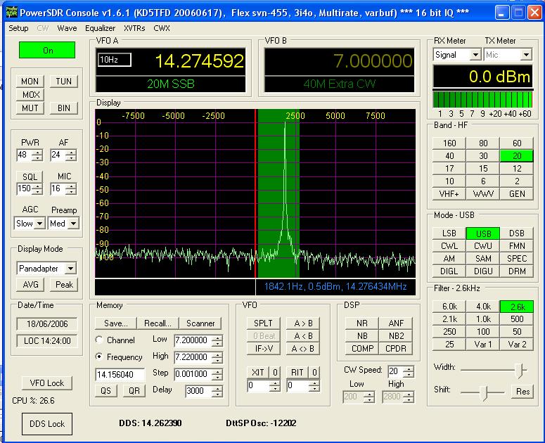
18th June 2006. The image above is of the LT2208 connected via a Xylo FPGA board over USB 2 to PowerSDR. The input signal level is 0dBm and we have about 100dB of dynamic range. Thanks to Bill KD5TFD for modifying PowerSDR to take the 16 bit data from the LT2208.
The Verilog code in the Xylo FPGA implements a fixed NCO on 25.00MHz and multiplies the 16 bits of data from the LT2208 alternately buy 1 or or -1. This is followed by a CIC filter that decimates the data by 2048. Since the LT2208 is clocked at 100MHz this results in a data rate of approximately 48.8kHz.
Next we will implement a CORDIC based NCO to provide tunable frequency control plus a half band filter to follow the CIC. Assuming this will all fit in the Xylo FPGA! If not we will have to wait for the OZY board to do further testing.
The Verilog sofware for the FPGA is being written using the free web version of Altera's Quartus II V6.0 software
Phil...VK6APH
